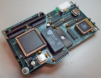
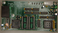
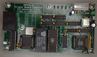
Here's what the bare PCB looks through 5-diopter magnification:
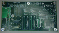
PCB Top Layer |
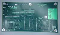
PCB Bottom Layer |
Satisfied with EPCB's work, I went to work "populating" the PCB—that is, installing components. As with most everything else, there is usually a procedure to be followed and assembling POC V1 was no exception. Lots of experience has taught me that it is best to install the most difficult components first, followed by the smallest, followed by the most expensive. With this procedure, if you goof up things, such as installing something backwards, you have a better chance of recovering from your error. At worst, you're less likely to waste expensive parts. So the first step was to install the SRAM, an SOJ-32 package with 50 mil pin spacing that would require reasonably precise soldering to avoid making a big mess. Here's what the PCB looked like after I had soldered the SRAM in place:
Although the SRAM's pins are on 50 mil centers, manual soldering isn't too difficult. I clamped the PCB to the bench and applied liquid solder flux to the PCB pads. Aside from its usual purpose, the flux helps to keep the part in place while soldering the first pin. Using a 40 watt iron equipped with an 0.032 inch chisel tip and set to high heat, I soldered the diagonally-opposite corner pins, using 63/37 rosin core solder. The technique is to put a drop of solder on the iron's tip, hold the part in place with tweezers, and then touch the tip to both the pin and the pad on the PCB, and keep it there until the solder and the reflow on the pad run together. Remove the tip and let the joint cool. Repeat for the other pin and the part is secured in place.
After a second check to verify that the part was correctly installed, I thoroughly cleaned and tinned the soldering iron tip and then soldered the remaining pins using a drag technique. With this technique, I don't attempt to avoid bridges, as they are readily cleaned up with desoldering braid. The key to a successful conclusion is to not get carried away with the amount of solder on the iron's tip. You want just enough to keep wetting the pins as you go, without too much build-up. If you do get a bridge, clean and tin your iron's tip and use it to press the desoldering braid down on the bridge. The braid will soak up the solder and you should have a nice, clean joint.
Incidentally, all SMT packages are designed to be soldered in reflow ovens, a process that exposes the part to a temperature around 450° F or 218° C. Therefore you need not worry about damaging the part while manually soldering, as long as you don't take too much time. Keeping your iron's tip hot and clean helps speed along the process. I've also had success in salvaging SMT devices using a heat gun to desolder them.
After a close visual inspection of my soldering handiwork, I tested for continuity and shorts at every pin, which checked out okay. I also metered between Vcc and ground to make sure that the soldering process didn't create a short. The continuity and short checks are especially important with SOJ type packages, as the point of contact between the pins and PCB pads is under the part, where it can't be readily inspected.
With the SRAM out of the way, I continued with populating the PCB, As everything else was through-hole, the rest of the task was straightforward. Here's a picture of the unit with all soldering completed but no plug-in components installed:
While POC V1 was in the "semi-populated" state, I metered between Vcc and ground once more to check for a possible short. The meter indicated that something wasn't right, as the DC resistance, which should have been very high, wasn't. Careful examination of the unit revealed that I had inadvertently installed one of the electrolytic capacitors backwards. After removing and reinstalling it the right way the Vcc–to–ground check was okay.
Here's what the finished unit looked like with all components installed:
With assembly completed, there was but one thing left to do, and that was to see POC V1 would go or blow. Needless to say, I was hoping for the former—not the latter!
Previous Page Home Next Page
