As earlier noted, I decided to use a four-layer PCB. In this type, there are two inner layers, as well as a top and bottom layer. The top and bottom layers are where the circuitry is placed, and the inner layers distribute power (Vcc) and ground to everything. Any pin on any chip or other device can be connected to one of the inner layers. Surface-mounted (SMT) devices can be connected to the inner layers by placing via (pass-through holes) on the SMT pads requiring such connections and telling the PCB layout software to connect the via to the desired layer. The use of the inner layers in this fashion eliminates the need to route Vcc and ground to each device, allowing parts to be packed closely together. The resulting denser board layout produces shorter signal paths, which aids in achieving satisfactory performance at high clock rates.
A corollary benefit of having the inner ground layer is that it assists in eliminating a phenomenon referred to as ground bounce, which if present can greatly upset circuit operation. The presence of the power and ground layers prevents crosstalk between the top and bottom layers, which effect can result in instability in cases where traces on the top layer are coincident to traces on the bottom layer. Also, due to their physical proximity, the inner power and ground layers act as a large bypass capacitor and thus assist in suppressing switching noise generated by the various chips. While this characteristic doesn't eliminate the need for decoupling capacitors, when combined with the capacitors, the bypassing effect of the power and ground layers results in a very "quiet" circuit.
Express PCB (EPCB) offers several different services to board designers, differing in maximum board size, maximum number of holes, and in some cases, presence or absence of solder masks and silk screening. One these services is called ProtoPro Four-Layer, which was the service I chose for POC V1. ProtoPro boards can be up to 21 square inches in size, may have a maximum of 650 holes and may have routed (irregular) edges. Finished boards include solder mask and silk screening, which means these boards are like regular production items but are produced in a fixed quantity of four and at a fixed price.
Included with the EPCB software is a board layout CAD program that can be used to design both two-layer and four-layer boards. It is possible to link a board layout to its corresponding schematic, which feature aids in producing an error-free layout. If the schematic was drawn with a program other than EPCB and is able to export its netlists, it can be indirectly linked to the EPCB board layout program by importation of the netlists. Something EPCB doesn't have is an autorouting function to aid in trace placement, which for a beginner can be a bit of a daunting task if the design has any complexity to it. Here, almost more than anywhere else in hobby computer design, knowledge of and experience with high speed electrical circuits is a big aid to producing a functioning and stable unit.
Computer circuits switch at very rapid rates and logic devices expect to see sharply defined voltage transitions at their inputs. As seen on an oscilloscope, the ideal voltage transition form is rectangular with an almost indiscernible rise and fall time. Deviations from this idealized form occur due to reactive effects in the circuit: distributed (parallel) capacitance and series inductance. As the operating frequency is increased, reactive effects rapidly mount and eventually a point is reached where the circuit will no longer function. Distributed capacitance tends to increase the signal rise and fall time, causing deviations from the idealized rectangular switching waveform. Given sufficient distortion, the affected logic device may become momentarily unstable as the input signal passes through an ambiguous area of the device's switching characteristic.
Series inductance causes signal propagation delay that can skew timing to a point where different parts of the circuit that are supposed to be operating on the same clock don't see the same rise and fall of the clock. If inductance is sufficient, signal amplitude will be markedly reduced, possible preventing the voltage transitions seen at a device's input from satisfying the device's switching requirements. Inductance, if present in sufficient amounts in power and ground circuits, will reduce the effectiveness of decoupling capacitors, causing a significant rise in circuit noise. In some cases, distributed capacitance in combination with series inductance may result in circuit resonance, which can cause complete failure at certain Ø2 clock rates.
Reactive effects can be mitigated by keeping circuit traces as short as possible and by using the most linear path possible. This was an aspect of my board layout into which I invested quite a bit of time. I wanted it to work right on the first try.
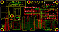
Here's what the board layout looked like as seen in the EPCB CAD program:
Items of note are:
- Image colors and markings are as follows:
- Red: top layer;
- Green: bottom layer;
- Yellow: silk screening;
- Blue: board perimeter;
- +: power (Vcc) inner layer connection;
- -: ground inner layer connection.
Not visible are the inner layers, which although viewable within the CAD program, are not usually of interest in most designs.
- The board is 6 inches side-to-side and 3.25 inches top-to-bottom,
equal to 19.5 square inches. The maximum permissible ProtoPro
area is 21 square inches. It should be apparent from viewing the
layout that I could have made the unit smaller by eliminating some of
the silk screen text (e.g., the BCS Technology Limited banner).
However, the cost for ProtoPro boards is the same regardless of the
board size, number of holes (as long as the hole count doesn't exceed
650), edge routing, etc. In any case, the density is good where it matters.
- All signal traces are 0.006 inches in width, a size that is only available with EPCB's four-layer service. Signal circuit via are 0.026 inches in diameter with a 0.008 inch hole, also a size only available with the four-layer service. These small sizes are a considerable aid in achieving good board density, as it usually isn't necessary to dog-leg a trace adjacent to a via to avoid interference. The default spacing on all traces is 0.025 inches.
- Traces that connect decoupling capacitors to their respective chips are at least 0.030 inches wide, although a narrower trace would be adequate. I was generous with this size to guarantee that DC resistance would not affect a decoupling capacitor's anility to do its job.
- There are no top and bottom filled planes (aka "ground pours"), except at the TIA-232 jack (the filled planes are not shown in the layout image). Filled planes greatly increase distributed capacitance, and will adversely affect the system's performance at higher clock rates. The filled planes at the TIA-232 jack are there to reduce EMI radiation and have no effect on circuit performance.
- I worked out an "ordered" component placement to "idealize" the layout. A basic rule of PCB design is to place components that are connected together as close together as possible. In the case of a computer PCB, the idealized layout will also keep the address and data bus traces as short as practical. I attempted to do so by placing the components with the most connections to the buses as close to the microprocessor (bottom right hand corner) as possible. Hence the SRAM is immediately to the MPU's left, followed by the EPROM, followed by the WDT, followed by the DUART. I placed the glue logic above these chips to aid in producing a short and direct routing of address bus, data bus and control signal traces (especially /IRQ).
- The two resistor networks that act as pull-ups for MPU signals, such as IRQB and NMIB, are as close to the MPU socket as possible (on the right side). Again, short traces are a virtue in reducing the distributed capacitance that these resistors have to charge to Vcc.
- The TO-92 package to the right of the MPU is the DS1813 econo-reset, which I previously described.
- The rectangular object at the top right hand corner of the board is the power input connection. It accepts a standard 5.25 inch disk drive connector found on PC power supplies. A better choice for this item would have been the smaller Berg connector used on 3.5 inch floppy disk drives. However, I didn't have a source for those at the time when I did this layout. There is also a "power good" LED to let me know when the power is on (the power supply I am using makes no discernible noise when running).
- The rectangular object at the left hand end of the board is the dual 8P8C (or RJ-45) jack to which TIA-232 (aka RS-232) connections are made. The A designation refers to the console port.
- The "expensive" chips, such as the MPU and the WDT, are socketed. I wasn't about to solder any of this stuff into the board until I knew to a certainty that the circuit would function. All of the glue logic is soldered though, as it is cheap. Socketing the glue logic would only increase distributed capacitance and in some cases, reduce reliability.
The above image is slightly distorted because it was photographed through 5-diopter magnification—my digital camera doesn't do good closeups on its own. You'll see more of this in other images. I need to break down and invest in a better camera! (NB: I replaced my camera in late 2014. The new one does very good closeups.)
The result of the layout and positioning verification step was to slightly relocate a few items to better facilitate assembly. Following a final check of everything, I submitted the PCB file to EPCB to be manufactured. The entire process is done through a secure Internet connection, using a credit card to pay for the finished goods. Turnaround time for the ProtoPro service typically works out to five business days.
By the way, remember when I said there was a design error in the circuit? Well, it went to EPCB in the submitted file. However, don't fret! The unit "sort-of worked" on the first try—after I fixed a very obscure layout error that was also present.
Previous Page Home Next Page


