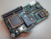
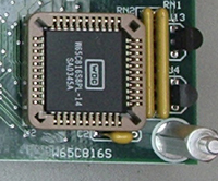
Eventually, I will move on to POC V2, which will be designed around programmable logic and larger amounts of memory. POC V2 will be a stepping stone to a full-featured design on which I hope to achieve the goal of being able to support preemptive multitasking. For now, only POC V1 will be discussed.
Design Criteria
That POC V1 is a "proof-of-concept" design dictated just how complicated it had to be. I had to avoid concocting too ambitious a design, as debugging an overly-complex unit would be difficult with the resources available to me, although since I started I have acquired better test equipment to diagnose hardware issues. On the other hand, this first design did have to be capable of doing more than merely using electricity and scribbling some text on a display screen. Yet another wish was to get the unit to be stable with an 8 MHz Ø2 clock. Whether that would be possible would depend on a number of factors—primarily logic propagation delays, and how well I did the physical layout and assembly. As logic delays can sabotage timing, and needlessly limit the maximum speed at which the circuit could be run, I made the decision to use 74AC logic, as it is fast and readily available in standard DIP packages.Firmware is required to do anything with any computer at power-on. Otherwise, the computer is little more than an electrically powered desk ornament. Therefore, I decided to provide POC V1 with a basic input/output subsystem (BIOS), interrupt handlers, reset handler, a Motorola S-record loader and a machine language (M/L) monitor, all to be packed into 8 kilobytes (KB) of ROM. An M/L monitor is indispensable for low-level debugging, so I decided I would build as much functionality into it as was possible. I'll discuss at length firmware development on a following page.
Hardware
With some design goals established, the next step was to pick the hardware to achieve them. As I previously mentioned, I decided to use a dumb terminal for communication with the POC. The particular terminal I like is the WYSE 60, which in the world of host-based computer systems (especially UNIX), was the number one choice of system integrators for many years. The WYSE 60, in addition to displaying monospaced text, has box graphics capability, and uses TIA-232 (aka RS-232) for communication with its host system. In my design, I needed to be able to connect the terminal and also link the POC to my UNIX software development machine, on which I have my 65xx cross-assembler. Hence there are two TIA-232 ports on the SBC, each of which can run at speeds up to 115.2 kilobits per second (Kbps). However, the maximum rate supported by the WYSE 60 is 38.4 Kbps, so that is how fast the primary or "console" port is run. The secondary or "auxiliary" port is also run at that speed, primarily for programming convenience, but also to prevent data transmission errors that might occur at higher speeds.I needed some sort of timekeeping mechanism to generate evenly spaced interrupts ("jiffy" interrupts), as well as programmable time delays. The logical choice was to use a battery-backed real-time clock (RTC) with a watchdog timer (WDT). In microcontroller applications, a WDT is often used to restart the system in the event of fatality. In this application, I planned on using the WDT to generate an interrupt at 10 millisecond intervals (100 IRQs per second) to drive a 32 bit uptime counter and a 16 bit programmable time-delay counter. That interrupt rate wasn't something that just came out of my hat. UNIX systems have, for many years, used a 100 Hz jiffy interrupt rate that, among other things, is involved with job scheduling.
Aside from selection of the MPU itself, there are a variety of ways to approach the design of this sort of system. Following some serious thinking, I chose the following devices (starting at the lower right hand corner of the above illustration):
- 128k x 8 fast static RAM (SRAM) in an SOJ32 surface mount (SMT) package.
- 27C256 32k x 8 EPROM in a DIP28 package. Note that a 28C256 EEPROM could have been substituted. I went with the 27C256 because I had some laying around.
- Maxim DS1511Y real-time clock with watchdog timer in an EDIP28 package.
- NXP 2692A dual asynchronous communications interface adapter (ACIA or DUART—dual universal asynchronous receiver/transmitter) in a PLCC44 package.
- Maxim MAX238 TIA-232 quad line driver in a DIP24 package.
- 74AC glue logic.
The MPU's clock oscillator output is fed to a D-type flip-flop and the Q output of the flop produces the actual Ø2 signal, resulting in a very sharply defined clock pulse. The '816 is somewhat fussy about Ø2's symmetry and rise and fall time—the flop produces a 2-3 nanosecond rise and fall, well within the '816's requirements. This arrangement means Ø2 is one half the frequency of the clock generator. The plan was to start with Ø2 at 1 MHz (2 MHz clock oscillator), and assuming the POC worked, increase Ø2 until the point of instability was noted, which would give me an idea as to how well I did my design homework.
The Maxim DS1511Y real-time clock (RTC) has a 24 hour clock (with alarm), a calendar, a watchdog timer and several other features that will be useful in the future. The date and time registers read out in binary-coded decimal (BCD), which reduces the complexity of conversion to or from ASCII. Embedded in the RTC is a lithium power source so it can keep time when the system is powered down.
An important hardware requirement that is sometimes overlooked by the hobbyist is that of having a safe, reliable and clean power source. I chose an old ATX PC power supply to run the POC, using one of the disk drive Molex power connectors. PC power supplies generally produce clean and stable DC, and do not expose dangerous voltages to the experimenter. They also incorporate a "crowbar" circuit that rapidly cuts off power in the event a fault occurs.
Construction
Having decided on what hardware to use, the next question to be resolved was the construction method. Projects of this type are either built on perf board using wire-wrap and/or point-to-point soldered connections, or on a printed circuit board (PCB). In years past, I would have wire-wrapped something like this, primarily because of the costs involved in designing and producing PCBs. The availability of reasonably priced PCB prototyping services and inexpensive or free design software has changed the picture. For that reason, as well as the use of the SOJ32 SRAM package (and my not-so-good eyesight), I decided to go with a PCB. Aside from greater ease of assembly, using a PCB would allow me to produce a dense layout that would be less likely to become unstable with increases in the Ø2 rate. I also made the decision to use a four-layer PCB, with internal power and ground layers. Doing so would simplify board layout and would aid in keeping the overall circuit noise level down to a dull roar.Both the MPU and DUART are available in DIP40 and PLCC44 packages. In the case of the DUART, some chip features are not available in DIP40 due to the reduced available pin count. In general, the PLCC package consumes less space than the DIP package, and owing to the grid-like pin arrangement of the PLCC socket, can result in shorter traces and a denser layout. However, the close grid layout can complicate trace routing (the only way out for traces connected to the inner pins is past the outer pins) and, if not done right, will lead to localized high distributed capacitance, which can distort signal waveforms and trigger instability. To settle the issue in my mind, I did PCB layouts with both package types. The final layout with PLCC packages was about 20 percent smaller in overall size, and trace routing for the address and data buses was more compact.
I choose ExpressPCB (EPCB) for my PCB source. I don't recommend EPCB for volume production, however they are fine with the small quantities typically used by hardware development engineers like me and hobbyists. EPCB provides Windows-based CAD software to design the circuit and lay out the board. The software does not produce industry-standard Gerber files, nor does it have the capabilities of a more sophisticated package such as Kicad. The use of a proprietary format in the design files is obviously a form of vendor lock-in and is one of the reasons why EPCB, in my opinion, is not a good choice for volume production—their pricing structure is not particularly attractive, as well. That said, EPCB's quality and service have been exemplary and I will continue to use them for low volume applications of this type.
Previous Page Home Next Page

